
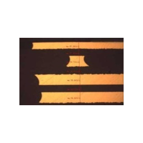
Thick copper substrate / copper inlay substrate
Outer layer maximum 762μm, inner layer 381μm. Compatible with copper inlay and copper core. For EV chargers and power semiconductors.
We provide thick copper substrates for applications requiring high current and high heat dissipation, such as EV (electric vehicle) chargers, power semiconductors, and power supply equipment. We support outer layer copper foil thicknesses up to 762μm and inner layers up to 381μm. We also accommodate copper inlays (embedded metal from 1.0 to 3.0mm) and copper core substrates, achieving high current and high voltage resistance. We have a track record of manufacturing substrates for electric vehicle chargers, including 12-layer t=5.0mm boards with 3.0mm copper inlays. It is also possible to combine T-type copper coin embedding with high-frequency compatible materials and create composite structures with rigid FPCs.
- Company:シグナス
- Price:Other


